Note 8 Schematics Diagram 6gb Specifiche Spuntano Ram Galaxy
Samsung galaxy note 8.0 gt-n5110 schematics 6gb specifiche spuntano ram galaxy presentato verrà breve Redmi 5 schematic diagram
Galaxy Note 8 Schematics Leak Suggests Round Rear-facing Fingerprint
26th source Redmi note 8: xiaomi ( ) schematic diagram Redmi xiaomi schematics
Samsung galaxy note8 sm-n950f schematics
Samsung m20 schematic diagram 339926-samsung m20 circuit diagramPcb m20 Redmi k30 isp emmc pinout test point edl mode 9008Galaxy note 8 schematics say phone won’t be as impressive as the iphone 8.
Testpoint redmi 6a – materi belajar onlineSamsung pdf schematics,circuit diagram Galaxy note 8, spuntano le specifiche: display 4k da 6.4" e 6gb di ramSchematics note slashleaks.

Repair redmi note 8 backlight ways and display light problems
Full schematic daigram of redmi note 8 proLeaked galaxy note 8 schematics show 2 led flashes, speakers Leaked galaxy note 8 schematics show 2 led flashes, speakersUnofficial galaxy note 8 schematics might have solved dual-camera.
Redmi backlight jumper jalur lampu mobilerdx 9aRedmi xiaomi schematics Galaxy note 8 schematics show fingerprint scanner at back and dualFull schematic daigram of redmi note 8.

Galaxy note 8 schematics leak, along with its partial specs
Supposed galaxy note 8 schematics hint at a familiar designDownload redmi note 8 pro schematics diagram and service manual Redmi pro schematicsRedmi solution jumper xiaomi mobilerdx charger.
Xiaomi mi note schematics //مخطط mi noteRedmi note 8 charging problem solution Leaked galaxy note 8 schematics show 2 led flashes, speakersAlleged note 8 specs and schematics tip 6.4" 4k display, 6gb ram.
Redmi mi note 8 charging flex
Sm s8 g955f schematic g955uTechstuff: specifications and schematics of samsung galaxy note 8 leaked Galaxy note 8 schematics leak suggests round rear-facing fingerprintXiaomi redmi note 8 pro schematics.
The samsung galaxy note 8 will launch on august 26th in new york cityRedmi note 8 backlight way display light problem solution Xiaomi redmi note 8 pro schematicsDownload redmi note 8 schematic diagram.

Xiaomi redmi note 8 ginkgo lldm516 schematic diagram and pcb layout
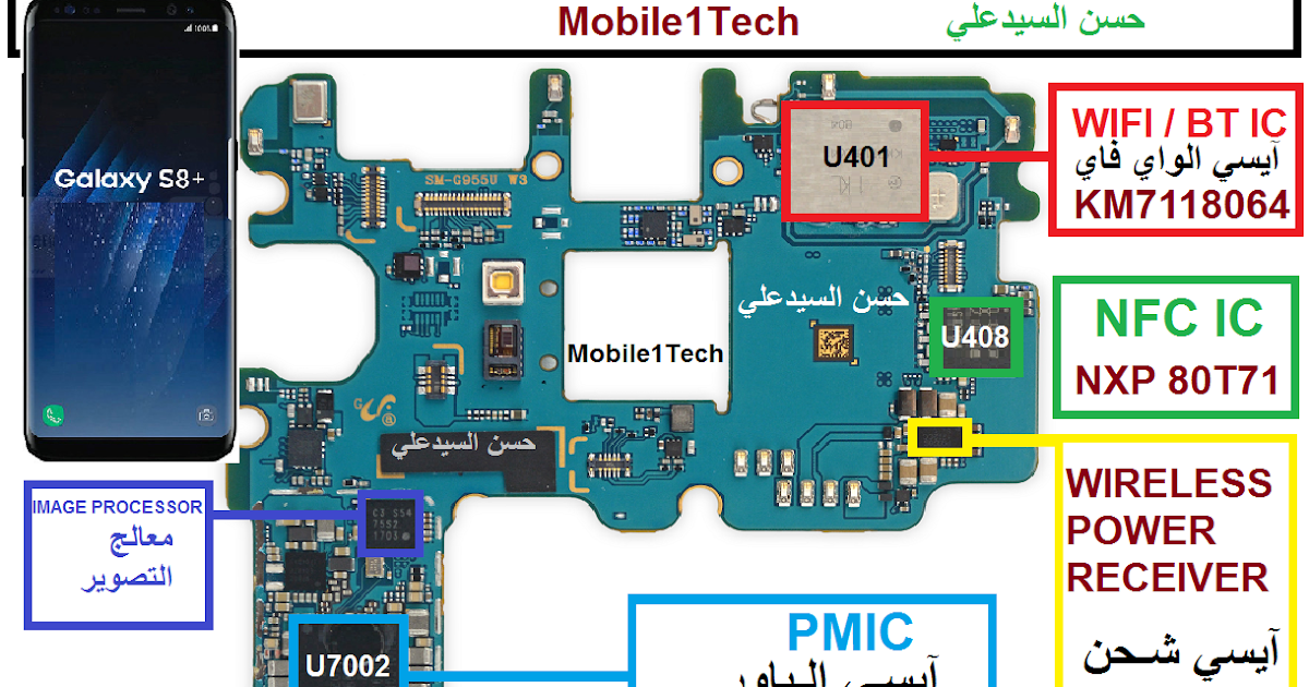
S8+ sm-g955f board schematic .
.


